Skip to content
-
-
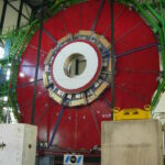
One of the discs of CMS being lowered down to the experimental cavern.
-
-
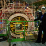
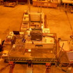
Panja in front of the CMS detector under construction in the experimental cavern.
-

-
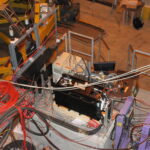
Installing the pixel detector into CMS.
-

-
One of the CMS endcaps.
-
-
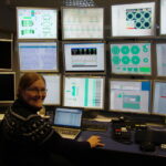
Panja in front of the CMS detector control system.
-
-
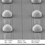
SEM image of the CMS pixel detector solder bumps.
-
-
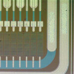
Pixels of the CMS pixel detector.
-
-
Corner of the CMS pixel detector.
-
-
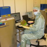
CMS pixel detectors being measured at the probe station.
-
-
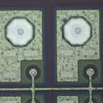
A lithography mask.
-
-
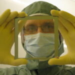
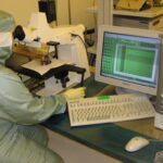
Tatyana checking the CMS detector wafer under the microscope.
-
-
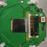
Esa holding the CMS pixel ROC wafer.
-
-
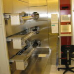
Micronova processing furnace.
-
-
Silicon wafers coming out of the processing furnace.
-
-
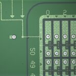
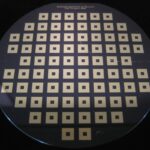
HIP pad detector wafer (version 1).
-
-
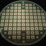
HIP pad detector wafer (version 2).
-
-
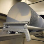
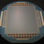
Large HIP silicon strip detector.
-
-
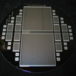
Small HIP silicon strip detectors.
-
-
Corner of the HIP strip detector.
-
-
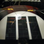
SiBT on the large XY-table at CERN H2 beam line.
-
-
SiBT at CERN H2 beam line in front of CMS HCAL and ECAL.
-
-
MCz detector module with CMS APV readout.
-
-
CMS MSSD detector attached to SiBT cold box plate.
-
-
Detectors inside the SiBT cold box.